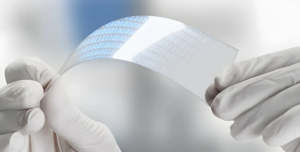
Graphene printing technology can help create electronic circuits that are low-cost, flexible, highly conductive, and water-resistant.
This newly developed nanotechnology “will bring great value to washable and self-cleaning wearable electronics that are resistant to stains, ice formation, and biofilm growth.”
“We use inexpensive graphene, printed with an inkjet printer, and then convert it with a laser to create functional, usable materials,” said Jonathan Claussen, assistant professor in the Department of Mechanical Engineering at Iowa State University.
Claussen’s article in the journal Nanoscale describes how he and his nanotechnology engineering team used inkjet printing technology to create electronic circuits on flexible materials. In this case, the ink is made of thin graphene flakes – a material of the future with extremely high electrical and thermal conductivity, exceptional durability, stability, and biocompatibility.
Freshly printed graphene flakes initially have relatively low conductivity and must be processed to remove non-conductive binders and weld the small flakes together, enhancing their conductivity and making them functional for use in electronic devices or sensors.
Post-print processing is usually done with heat or chemicals. However, Claussen and his team developed a rapid-pulsing laser that can achieve the same effect without damaging the printed surface – even when the surface is paper.
They also discovered another application for this laser technology: turning water-attracting (hydrophilic) printed graphene circuits into water-repellent (superhydrophobic) circuits.
“We shrank the surface pattern of the printed graphene flakes. The laser arranges the flakes vertically, stacking them like tiny pyramids. That is what creates the water repellency,” Claussen explained.
He added that the laser’s energy density can be tuned to change the water repellency level and conductivity of the printed graphene circuits.
This opens up countless opportunities for future electronic devices and sensors.
“One of the things we want to develop is anti-biofouling materials,” said co-author Loreen Stromberg.
“This will eliminate buildup on the surface of biomaterials that can reduce the performance of devices, such as biological or chemical sensors.”
This technology also has potential applications in flexible electronics, washable textile sensors, microfluidics, drag reduction, de-icing, electrochemical sensors, and even in technologies that use graphene structures and electrical stimulation to produce stem cells for neural regeneration.
The researchers say more studies will be conducted to better understand how the nano- and micro-structures of printed graphene flakes can create water repellency.
This technology is currently being patented by Iowa State University and may be licensed to the startup NanoSpy Inc. for commercialization. NanoSpy – based on campus – is developing sensors to detect rod-shaped bacteria and other pathogens during plant processing.
Graphene printing, processing, and tuning technology will be extremely useful as electronic devices continue to be integrated into more and more applications.
