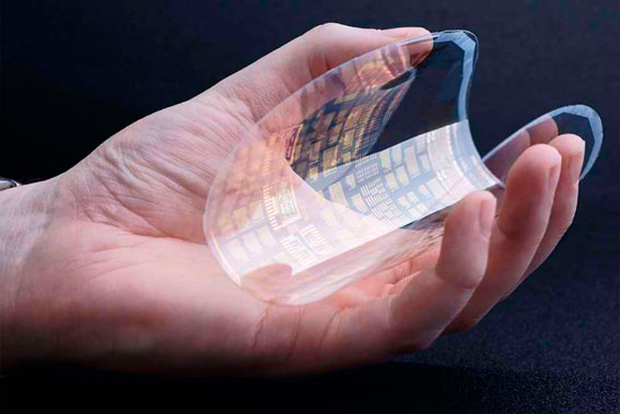
Graphene Photodetectors Integrated into Silicon CMOS Chips Could Herald a New Optoelectronic Era
Most modern long-distance data transmission relies on infrared laser light, which means that all terminal devices require an optical photodetector to convert optical signals into electrical ones. This week, scientists at the Vienna University of Technology have successfully created an infrared photodetector made of graphene. This remarkable material—already revolutionary across many industries—could transform how we build computers and computer networks.
There are two main advantages here, and the first is speed — orders of magnitude faster. The newly developed photodetector shows extremely low signal loss behind the graphene layer in terms of speed and response time (latency). Because of graphene’s unique atomic arrangement, its electrons are evenly distributed throughout the lattice, allowing them to move almost without resistance. As a result, when a photon strikes the material, the electrical signal appears almost instantly. The response of this new infrared photodetector is up to eight times faster than earlier models where graphene was fabricated separately from the chip.
The second major advantage of graphene is its astonishingly small size.
It is so compact that a single one-square-centimeter chip could theoretically host up to 20,000 of these photodetectors. This means that a high-resolution conversion array could allow a chip to receive up to 20,000 independent signal channels — at least in theory. Whether the chip can actually handle that many simultaneous channels, however, is an entirely different challenge.
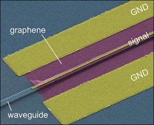
The biggest hurdle is not creating a graphene-based photodetector but integrating it into a chip.
You cannot simply swap out the photodetector and continue using the old chip as before. In many respects, an infrared converter must transform optical signals into a form that a computer can process efficiently. Multiple processors within a system need to communicate with each other faster and consume less power to fully take advantage of this technology.
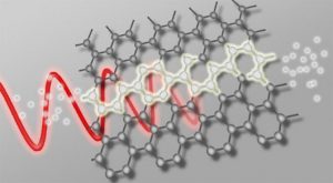
Graphene can absorb and convert nearly the entire light spectrum used in modern communication signals.
Traditional photodetectors generate electrons from a single wavelength of incoming light. Researchers have demonstrated that graphene is capable of absorbing a much broader spectrum — ranging from 1310 nm to 1650 nm. This means it requires a dedicated waveguide to direct the light efficiently into the detector.
The study from the Vienna University of Technology is one of three research projects on graphene’s light-absorption capabilities published in Nature Photonics this week, opening up surprising new applications for this wonder material. The research builds upon graphene’s fundamental physical properties, which make it a highly promising candidate for ultra-fast superconducting wires and next-generation optical converters.
The biggest limitation of graphene lies in its sensitivity.
While its conversion speed is exceptionally fast, its response to low-intensity light is rather poor — about ten times worse than its competitor, germanium. Nevertheless, researchers remain confident that they can develop a solution to overcome this drawback.
Even so, their chip has already set a new benchmark in the field of data transmission and signal conversion, paving the way for the next generation of optoelectronic technologies.
