As we know, most electronic components are traditionally made from silicon-based semiconductors. The technology for producing silicon semiconductors has completely transformed the electronics industry. In fact, the world’s largest hubs for electronic device manufacturing, computer technology, and semiconductor chip research are collectively known as Silicon Valley. This alone underscores the critical importance of silicon in today’s electronics industry. However, the latest research from scientists at the Norwegian University of Science and Technology may change the significance and influence of this technology.
In a recent study, researchers have developed a new type of semiconductor built on a graphene substrate, capable of overcoming the inherent limitations of silicon-based semiconductors, such as thickness and light obstruction. This new material is only one micrometer thick, extremely flexible and transparent, and its production cost is significantly lower compared to silicon-based semiconductors.
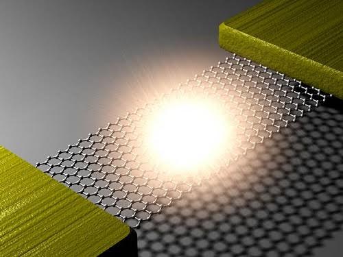
Graphene itself is a lattice of carbon atoms bonded in a hexagonal pattern, forming long, sheet-like structures. These bonds are exceptionally strong, the material conducts electricity very well, and its sheet-like structure gives it an extremely thin profile.
To create this new semiconductor material, scientists implanted gallium atoms onto the graphene substrate in a vacuum chamber. The gallium atoms adhere to the graphene lattice, forming gallium droplets. Next, arsenic atoms are introduced, which are absorbed into these gallium droplets. This process is repeated multiple times until the gallium droplets form ultra-small nanowires, approximately one micrometer in height. Finally, the graphene substrate is removed, leaving behind the new semiconductor material.
